- 您现在的位置:买卖IC网 > Sheet目录17358 > NCP1014STBUCGEVB (ON Semiconductor)EVAL BOARD FOR NCP1014STBUCG
NCP1010, NCP1011, NCP1012, NCP1013, NCP1014
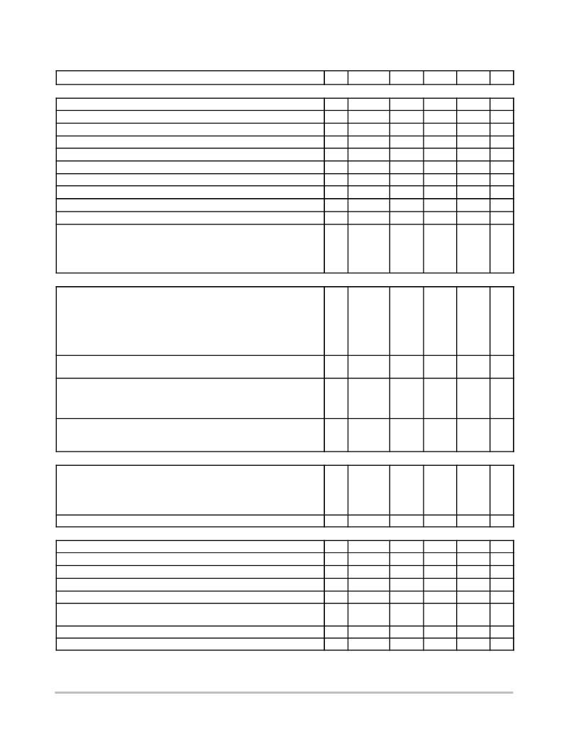
ELECTRICAL CHARACTERISTICS (For typical values T J = 25 ? C, for min/max values T J = --40 ? C to +125 ? C, Max T J = 150 ? C,
V CC = 8.0 V unless otherwise noted.)
Rating
Pin
Symbol
Min
Typ
Max
Unit
SUPPLY SECTION AND V CC MANAGEMENT
V CC Increasing Level at which the Current Source Turns--off
V CC Decreasing Level at which the Current Source Turns--on
Hysteresis between VCC OFF and VCC ON
V CC Decreasing Level at which the Latch--off Phase Ends
V CC Decreasing Level at which the Internal Latch is Released
Internal IC Consumption, MOSFET Switching at 65 kHz (Note 2)
Internal IC Consumption, MOSFET Switching at 100 kHz (Note 2)
Internal IC Consumption, MOSFET Switching at 130 kHz (Note 2)
Internal IC Consumption, Latch--off Phase, V CC = 6.0 V
Active Zener Voltage Positive Offset to VCC OFF
1
1
1
1
1
1
1
1
1
1
VCC OFF
VCC ON
--
VCC latch
VCC reset
ICC1
ICC1
ICC1
ICC2
Vclamp
7.9
6.9
--
4.4
--
--
--
--
--
140
8.5
7.5
1.0
4.7
3.0
0.92
0.95
0.98
290
200
9.1
8.1
--
5.1
--
1.1
1.15
1.2
--
300
V
V
V
V
V
mA
mA
mA
m A
mV
Latch--off Current
1
ILatch
mA
NCP1012/13/14
NCP1010/11
0 ? C < T J < 125 ? C
--40 ? C < T J < 125 ? C
0 ? C < T J < 125 ? C
--40 ? C < T J < 125 ? C
6.3
5.8
5.8
5.3
7.4
7.4
7.3
7.3
9.2
9.2
9.0
9.0
POWER SWITCH CIRCUIT
Power Switch Circuit On--state Resistance
NCP1012/13/14 (Id = 50 mA)
T J = 25 ? C
T J = 125 ? C
NCP1010/11 (Id = 50 mA)
T J = 25 ? C
T J = 125 ? C
5
R DSon
--
11
19
22
38
16
24
35
50
Ω
Power Switch Circuit and Startup Breakdown Voltage
5
BVdss
700
--
--
V
(ID (off) = 120 m A, T J = 25 ? C)
Power Switch and Startup Breakdown Voltage Off--state Leakage Current
T J = --40 ? C (Vds = 650 V)
T J = 25 ? C (Vds = 700 V)
T J = 125 ? C (Vds = 700 V)
5
5
5
I DS(OFF )
--
--
--
70
50
30
120
--
--
m A
Switching Characteristics (RL = 50 Ω , Vds Set for Idrain = 0.7 x Ilim)
ns
Turn--on Time (90%--10%)
Turn--off Time (10%--90%)
5
5
ton
toff
--
--
20
10
--
--
INTERNAL STARTUP CURRENT SOURCE
High--voltage Current Source, V CC = 8.0 V
NCP1012/13/14 0 ? C < T J < 125 ? C
--40 ? C < T J < 125 ? C
NCP1010/11 0 ? C < T J < 125 ? C
--40 ? C < T J < 125 ? C
High--voltage Current Source, V CC = 0
1
1
IC1
IC2
5.0
5.0
5.0
5.0
--
8.0
8.0
8.0
8.0
10
10
11
10.3
11.5
--
mA
mA
CURRENT COMPARATOR T J = 25 ? C (Note 2)
Maximum Internal Current Setpoint, NCP1010 (Note 3)
Maximum Internal Current Setpoint, NCP1011 (Note 3)
Maximum Internal Current Setpoint, NCP1012 (Note 3)
Maximum Internal Current Setpoint, NCP1013 (Note 3)
Maximum Internal Current Setpoint, NCP1014 (Note 3)
Default Internal Current Setpoint for Skip--Cycle Operation, Percentage of
Max Ip
Propagation Delay from Current Detection to Drain OFF State
Leading Edge Blanking Duration
5
5
5
5
5
--
--
--
Ipeak (22)
Ipeak (22)
Ipeak (11)
Ipeak (11)
Ipeak (11)
I Lskip
T DEL
T LEB
90
225
225
315
405
--
--
--
100
250
250
350
450
25
125
250
110
275
275
385
495
--
--
--
mA
mA
mA
mA
mA
%
ns
ns
2. See characterization curves for temperature evolution.
3. Adjust di/dt to reach Ipeak in 3.2 m sec.
http://onsemi.com
5
发布紧急采购,3分钟左右您将得到回复。
相关PDF资料
L-07C1N0SV6T
CER INDUCTOR 1NH 0402
LM2594APDBCKGEVB
EVAL BOARD FOR LM2594APDBCKG
EEM15DTBN
CONN EDGECARD 30POS R/A .156 SLD
SJP7401-5/8-50-BLACK
LOOP BLACK 5/8" X 50YD X 0.11"
EEM15DTBH
CONN EDGECARD 30POS R/A .156 SLD
RE-1515S/H
CONV DC/DC 1W 15VIN 15VOUT
GSC05DRTH-S13
CONN EDGECARD 10POS .100 EXTEND
TAAD157M016G
CAP TANT 150UF 16V 20% AXIAL
相关代理商/技术参数
NCP1015
制造商:ONSEMI 制造商全称:ON Semiconductor 功能描述:Self-Supplied Monolithic Switcher for Low Standby- Power Offline SMPS
NCP1015_11
制造商:ONSEMI 制造商全称:ON Semiconductor 功能描述:Self-Supplied Monolithic Switcher for Low Standby-Power Offline SMPS
NCP1015AP065G
功能描述:交流/直流开关转换器 SELF-SUPPLIED MONOLITHIC SWITCHER RoHS:否 制造商:STMicroelectronics 输出电压:800 V 输入/电源电压(最大值):23.5 V 输入/电源电压(最小值):11.5 V 开关频率:115 kHz 电源电流:1.6 mA 工作温度范围:- 40 C to + 150 C 安装风格:SMD/SMT 封装 / 箱体:SSO-10 封装:Reel
NCP1015AP100G
功能描述:交流/直流开关转换器 SELF-SUPPLIED MONOLITHIC SWITCHER RoHS:否 制造商:STMicroelectronics 输出电压:800 V 输入/电源电压(最大值):23.5 V 输入/电源电压(最小值):11.5 V 开关频率:115 kHz 电源电流:1.6 mA 工作温度范围:- 40 C to + 150 C 安装风格:SMD/SMT 封装 / 箱体:SSO-10 封装:Reel
NCP1015ST100T3G
功能描述:电流型 PWM 控制器 MONOLTHC SWTCHR SMPS RoHS:否 制造商:Texas Instruments 开关频率:27 KHz 上升时间: 下降时间: 工作电源电压:6 V to 15 V 工作电源电流:1.5 mA 输出端数量:1 最大工作温度:+ 105 C 安装风格:SMD/SMT 封装 / 箱体:TSSOP-14
NCP1015ST65T3G
功能描述:电流型 PWM 控制器 MONOLTHC SWTCHR SMPS RoHS:否 制造商:Texas Instruments 开关频率:27 KHz 上升时间: 下降时间: 工作电源电压:6 V to 15 V 工作电源电流:1.5 mA 输出端数量:1 最大工作温度:+ 105 C 安装风格:SMD/SMT 封装 / 箱体:TSSOP-14
NCP102
制造商:ONSEMI 制造商全称:ON Semiconductor 功能描述:Low Dropout Linear Regulator Controller
NCP1027
制造商:ONSEMI 制造商全称:ON Semiconductor 功能描述:Power Factor Controllers
